ALTIUM · SINGLE-LAYER · 12 UNITS SHIPPED
A minimum-load board that lets a lab ATX supply start under near-zero draw. Full lifecycle: research, schematic, layout, fab, hand assembly. In production use at Thales.
- ORG
- Thales · CSP hardware team
- ROLE
- Sole designer · research → layout → assembly
- STAGE
- IN PRODUCTION · 17 units built
- STACK
- Altium · SolidWorks · PCBWay · FR4
Bench power supplies in the lab refused to start. Not the boards under test, the supplies themselves: press the switch, watch the rails come up for a few milliseconds, watch them latch off again. The board being tested drew too little current for its own power supply to regulate.
The workaround already in use was a 2 Ω 25 W power resistor alligator-clipped onto a spare rail. It worked, it dumped heat into the bench, and it was one loose clip away from shorting something expensive. I was handed the job of turning it into a real board.
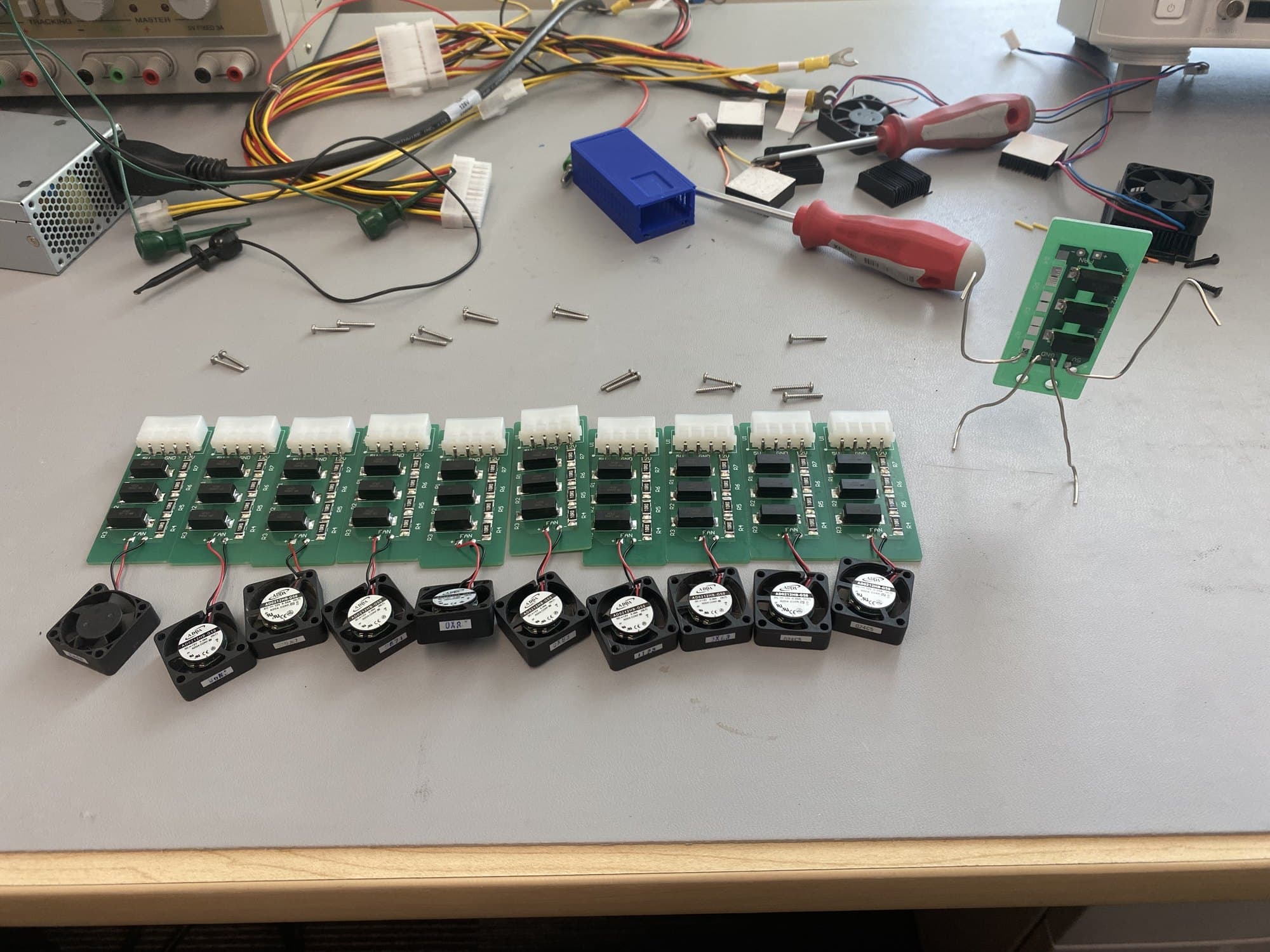
I hand-soldered seventeen of them. Twelve are in production PSU testing at the Plantation office; five went to Canada with my manager for his team.
A switching supply regulates by sensing its own output. Older group-regulated designs watch the 12 V rail, or a combined 12 V and 5 V sense. With near-zero load the feedback loop has nothing to settle against: the output overshoots, trips over-voltage or power-good protection, and latches off. That is why the datasheet lists a minimum load current per rail. Running below it is out of spec, not bad luck.
The board under test pulled 5 V only, to source USB VBUS. With no USB device attached it drew roughly 0.05 A— orders of magnitude under the supply’s stated minimum.
Before designing anything I loaded each rail with known resistances to find where startup actually failed, rather than trusting the number on the page.
| RAIL | LOAD | CURRENT | STARTUP |
|---|---|---|---|
| +5 V | 9.9 Ω | 0.51 A | Success |
| +5 V | 13.2 Ω | 0.38 A | Fail |
| +12 V | 9.9 Ω | 1.21 A | Success |
| +12 V | 13.2–37.7 Ω | 0.91 → 0.32 A | Unreliable |
The 5 V rail behaved exactly as specified: it started at its rated 0.5 A minimum and failed below it. The 12 V rail did not. It reported successful startups well under its 1 A rating, but not repeatably — the load test never pinned down a true 12 V minimum, and I would rather record that than invent a threshold.
What did give a clean answer was loading the rail with fans instead of resistors. Three fans populated started the supply reliably, fewer than three did not, and three fans draw a measurable 0.2425 A on 12 V — a real, reproducible figure to design against where the resistor sweep had given none.
I had been sizing a permanent bleeder — a resistor bank sitting across the rail forever, burning power for as long as the supply is on.
That reframed the thermal budget entirely: a load sized for a startup transient is a much smaller, cooler, cheaper thing than one sized to run forever.
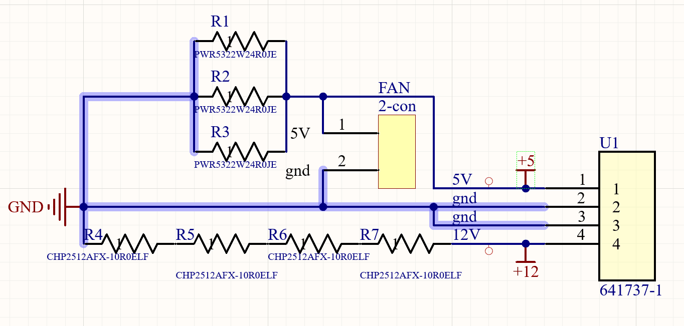
My first pass sized resistors at nominal rail voltage. That is wrong. A supply is allowed to sit anywhere inside its regulation band, and the minimum-current requirement has to hold at the low end of that band. Everything was resized across the full ±5% tolerance — [4.75 V, 5.25 V] and [11.4 V, 12.6 V] — so the load still clears minimum at the worst case.
| RAIL | PART | CONFIG | LOAD | TARGET I | PER-RESISTOR |
|---|---|---|---|---|---|
| +5 V | PWR5322W24R0JE · 24 Ω 3 W | 3 × parallel | 8 Ω | 0.625 A | 0.93 W |
| +12 V | CHP2512AFX-10R0ELF · 10 Ω 3 W | 4 × series | 40 Ω | 0.3 A | 0.85 W |
Parallel on 5 V to divide current, series on 12 V to divide voltage — either way the dissipation spreads across a field of parts instead of concentrating in one hot spot, and every resistor lands under a third of its 3 W rating.
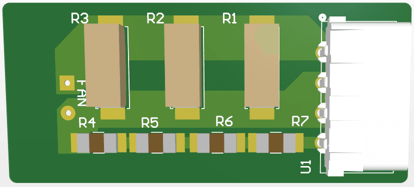
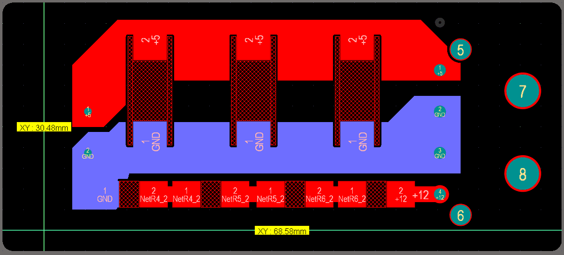
Two things changed during layout. The through-hole resistors I first picked turned out to be enormous once placed, so the 12 V bank moved to surface-mount chips and the board footprint dropped to under half its original size. The board also collapsed to a single copper layer, the only through-holes being the mounting legs of the TE 641737-1 connector.
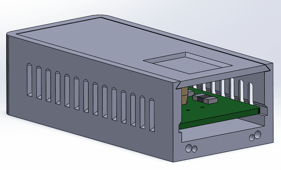
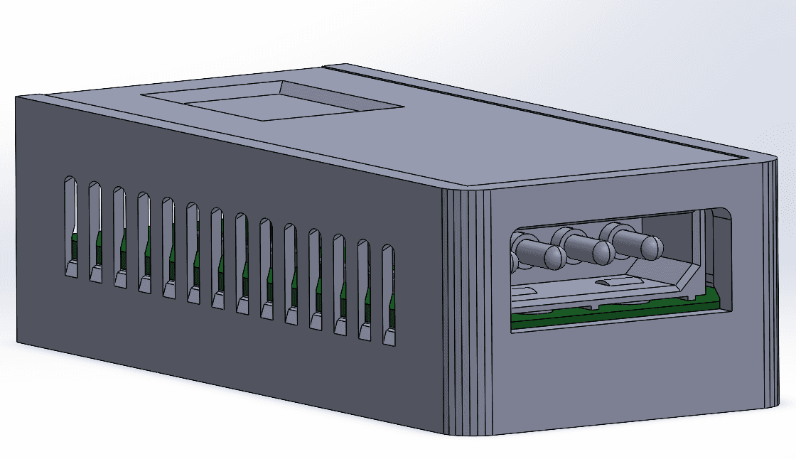
A bare board with exposed rails living loose in a test bench is an accident waiting to happen, so the board got a 3D-printed case — my first real SolidWorks work. Vented along the long face, open at the connector end, with a window over the resistor bank.
The boards arrived and they work — every time, which the alligator clip never did. But there is a real defect in the design and it is mine.
There are fan pads on the board, and I put them there as an optional convenience. In practice they are not optional. The board works because someone points a fan at it, not because I designed it to. At any meaningful current, ground pour, thermal vias and a decision about forced air belong in the layout from the first placement — not added after the thing runs hot.
An adjustable buck converter: 12 V in, 1.2–5 V out, with a trim pot on the feedback divider. The load board is a passive network — four resistors and a connector. This one is a switching regulator, with a control IC, an inductor, and a layout where component placement changes whether the circuit works.
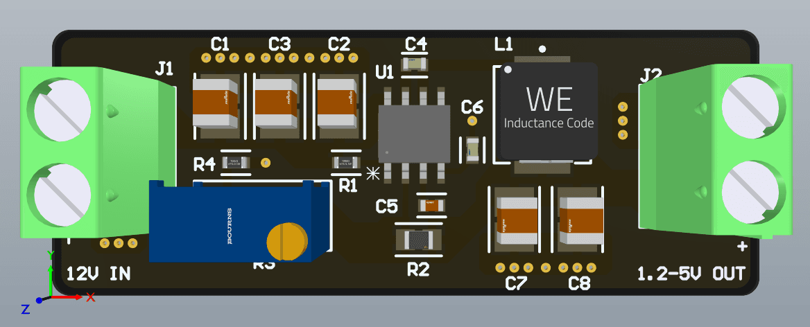
Review found a real problem with it, and it is a placement problem rather than a routing one: components that need short return paths are not close enough together. In a switching converter the current loops reverse direction millions of times a second, and the physical area those loops enclose behaves like an antenna — radiating noise, and adding inductance exactly where the design can least afford it. Placing those parts tight against each other is not a tidiness preference, it is the circuit working or not.
This needs a redesign before it is worth fabricating, and that redesign has not happened yet. I am showing it unfinished rather than leaving it out — it did the job I set it, which was learning the tool on something harder than a resistor bank, and it taught me a rule about placement I will not need to be told twice.
| ITEM | RESULT |
|---|---|
| Boards built | 17, hand-soldered |
| In production testing | 12 · Plantation FL |
| Sent to Canada | 5 · manager's team |
| Reliability | Starts the supply on every attempt |
| Known defect | Requires forced air at load |
This was the first board I took through the entire lifecycle on my own: purchase order, datasheet research, bench characterisation, schematic, trace rules, layout, part sourcing, fabrication order, receiving, hand assembly, an enclosure, and deployment to people who now depend on it. Every one of those steps had a way to fail that I had not met before.